The requirements of the readout electronics for CMS and other future high energy physics experiments are pushing the limits of present technology in terms of speed and the amount of data to transfer. All distributed front-end components have to run synchronously with the accelerator clock. Moreover, as the time of flight of particles has to be considered, clock and trigger delay have to be adjusted locally. Thus, the overall timing synchronization is a very challenging task.
The CMS Silicon Strip Tracker electronics essentially consists of two large blocks. The one-way readout chain transmits the measured data from the detectors to the control room. On the other hand, the bi-directional control chain has to deliver clock and trigger signals to each detector and exchanges control information between control room and front-end electronics such as configuration parameters or temperature monitoring.
In CMS, the read-out information is conveyed in analog state, while the control data are purely digital.
All signals are transmitted trough ![]() of optical fibers between front-end and control room.
On either end, the light information is converted to electrical signals and vice versa.
of optical fibers between front-end and control room.
On either end, the light information is converted to electrical signals and vice versa.
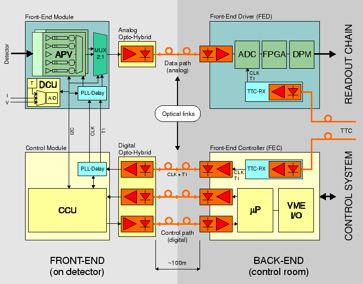 |
![[*]](crossref.gif) shows a sketch of the CMS Silicon Strip Tracker electronics.
The readout (top half) and control (bottom half) parts both include components close
to the detectors at the front-end (left half) and in the control room (right half).
shows a sketch of the CMS Silicon Strip Tracker electronics.
The readout (top half) and control (bottom half) parts both include components close
to the detectors at the front-end (left half) and in the control room (right half).
The Timing, Trigger and Control (TTC) System, which is a common development for all LHC experiments, takes care of clock and trigger distribution through optical fibers. Local receiver boards (TTCrx) provide these signals for the electronic modules. The Front-End Controller (FEC) takes this information, adds specific control signals received over its VME bus interface and sends these data to the front-end control module using a digital optical link. The Communication and Control Unit (CCU) interprets the received information and passes it on to the front-end module. Temperature, voltages and currents are monitored by the Detector Control Unit (DCU). Its data are transmitted to the CCU, which sends it back to the FEC. The PLL (phase-locked loop) delay chip is used for adjusting clock phase and trigger delay. In the readout path, the analog data coming from two APV25 front-end amplifiers are multiplexed onto a single line by the APVMUX chip and sent over the analog optical link. This data are then digitized and pre-processed by the Front-End Driver (FED), which receives the TTC clock and trigger signals as well. It buffers the incoming data and passes them on to a computer farm for further processing.
The CMS tracker uses the ![]() bus, which was developed by Philips [45], for
slow control in the front-end. Clock delay settings, configuration parameters
or monitored temperatures are transmitted over this bus. An address is assigned to each device
on this bus by tying dedicated input pads low or high.
Clock and trigger signals are transmitted with low voltage differential signaling (LVDS) levels.
In the control room back-end, there is no need for radiation hardness, and the electronic
modules are based on the industry-standard VME bus system.
bus, which was developed by Philips [45], for
slow control in the front-end. Clock delay settings, configuration parameters
or monitored temperatures are transmitted over this bus. An address is assigned to each device
on this bus by tying dedicated input pads low or high.
Clock and trigger signals are transmitted with low voltage differential signaling (LVDS) levels.
In the control room back-end, there is no need for radiation hardness, and the electronic
modules are based on the industry-standard VME bus system.
Several ASICs have been developed for the front-end electronics.
Since the chips are located close to the detector modules, they have to withstand
the same radiation levels. All ASICs are fabricated in the IBM
![]() deep submicron
CMOS process [37], which tolerates radiation far beyond the expected CMS levels.
deep submicron
CMOS process [37], which tolerates radiation far beyond the expected CMS levels.
The trigger line is not only used for the distribution of the first-level trigger, but
also for reset and calibration requests. The speed of the trigger line is
![]() with the valid symbols given in tab. .
A single logic 1 bit is a trigger, while 101 resets the target components and the calibration request
11 generates an internal calibration pulse in the APV chip.
This scheme implies that the minimum distance between two subsequent triggers is three clock
cycles, i.e. 1001 and a short dead time of
with the valid symbols given in tab. .
A single logic 1 bit is a trigger, while 101 resets the target components and the calibration request
11 generates an internal calibration pulse in the APV chip.
This scheme implies that the minimum distance between two subsequent triggers is three clock
cycles, i.e. 1001 and a short dead time of ![]() is introduced.
is introduced.
The various components of the Silicon Strip Tracker and the APV chip in particular will be discussed in detail in the following sections.