


Next: Internal Calibration
Up: APV25 Circuit Details
Previous: APSP
Contents
Multiplexer and Output Buffer
The sampled output of the APSP is sent to a single output line through a three-stage
multiplexer. Its principle is shown in fig. ![[*]](crossref.gif) .
Due to the staged multiplexing, the output order of the 128 channels does not correspond to the
natural channel order. The following calculation must be performed to retrieve the physical channel
number
.
Due to the staged multiplexing, the output order of the 128 channels does not correspond to the
natural channel order. The following calculation must be performed to retrieve the physical channel
number  from output sample number
  :
:
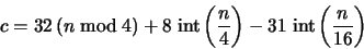 |
(4.1) |
Figure:
Principal structure of the APV25 multiplexer.
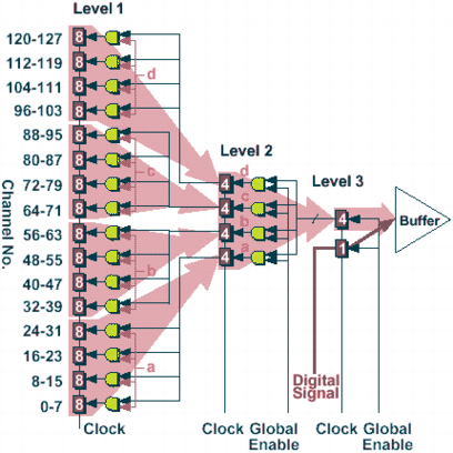 |
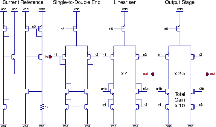
Fig. shows the multiplexer circuit.
Figure:
Schematics of the APV25 multiplexer.
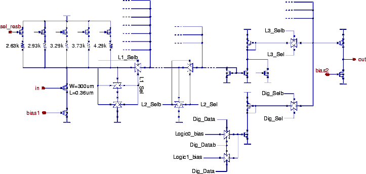 |
The APSP output voltage is first converted
into a current, which allows faster and more linear switching with less crosstalk.
The conductance of the input stage can be selected by switching on or off several
parallel resistors. This allows trimming of the multiplexer gain since the accuracy of chip internal
resistors is limited to about  . Channels which are not switched through have their
currents dumped into a dummy load. This is a waste of power but ensures that the voltages
are not affected by the switching procedure. To the bottom right of fig. ,
a circuit which inserts digital signals to the output line, is shown. The digital logic levels
are
. Channels which are not switched through have their
currents dumped into a dummy load. This is a waste of power but ensures that the voltages
are not affected by the switching procedure. To the bottom right of fig. ,
a circuit which inserts digital signals to the output line, is shown. The digital logic levels
are
 .
.
The analog gain at the output of the multiplexer is
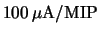 and the power consumption
of the whole multiplexer is
and the power consumption
of the whole multiplexer is  at the nominal input bias current of
  .
.
Figure:
Schematics of the APV25 output buffer.
 |
The output buffer shown in fig. finally amplifies the multiplexer
output current and splits it into differential channels.
Both output lines have an analog gain of  , resulting in a differential signal
of
, resulting in a differential signal
of  and differential logic levels of
  . The output buffer
power consumption is
. The output buffer
power consumption is  .
.
Next: Internal Calibration
Up: APV25 Circuit Details
Previous: APSP
Contents
Markus Friedl
2001-07-14