The APV25 includes an internal calibration generator [53], which
allows to check the functionality of each channel. The operational principle is to
apply a voltage step pulse ![]() to a series capacitor
to a series capacitor ![]() which is
connected to the preamplifier input. The
injected charge
which is
connected to the preamplifier input. The
injected charge ![]() is determined by
is determined by
| (4.2) |
The calibration pulses can be applied to one (or more) out of eight groups, each connected to
16 input channels of the amplifier. This selection is done by a mask register which is
programmable over the ![]() bus. Also the amplitude of the voltage step and thus the
injected charge can be adjusted. Moreover, the timing of the pulse can be adjusted
in steps of 1/8 of the system clock (
bus. Also the amplitude of the voltage step and thus the
injected charge can be adjusted. Moreover, the timing of the pulse can be adjusted
in steps of 1/8 of the system clock (![]() at
at ![]() ).
).
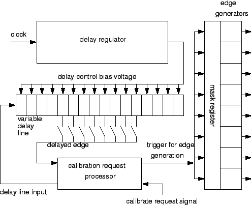
Fig.
![[*]](crossref.gif) shows the scheme of the APV25 calibration delay circuit
and the mask register for the selection of a group of input channels into which the
charge is injected.
The delay line has 16 stages with a tapping on one of the centered eight.
Each stage is implemented as a current-starved inverter followed by a Schmitt trigger.
A Delay-Locked Loop (DLL) circuit controls the current bias of the elements to ensure that the
total delay of all 16 stages equals two system clock periods.
shows the scheme of the APV25 calibration delay circuit
and the mask register for the selection of a group of input channels into which the
charge is injected.
The delay line has 16 stages with a tapping on one of the centered eight.
Each stage is implemented as a current-starved inverter followed by a Schmitt trigger.
A Delay-Locked Loop (DLL) circuit controls the current bias of the elements to ensure that the
total delay of all 16 stages equals two system clock periods.
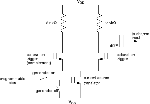
The output stage of the calibration circuit for a single channel is shown in fig.
.
With each calibration request signal, the state of the calibration trigger line is
toggled if enabled for that particular channel on the mask register.
The amplitude of the voltage pulse is adjusted with the programmable bias, driving
the current source of the complementary switching stage.
The current source can be completely switched off to avoid possible crosstalk.
The coupling capacitor is implemented in
between two metal layers of the routing lines on the chip.
The current source generates a nominal current between ![]() and
and ![]() ,
resulting in an injected charge of
,
resulting in an injected charge of ![]() to
to ![]() . However,
since both the resistors defining the amplitude of the voltage step and the capacitor
have considerable tolerances, the charge is not very well defined.
. However,
since both the resistors defining the amplitude of the voltage step and the capacitor
have considerable tolerances, the charge is not very well defined.
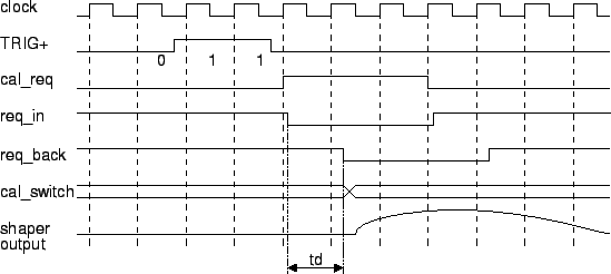
Fig.
shows the timing of the APV25 internal calibration.
A calibration request (cal_req) is detected when a 11 symbol appears on the trigger line.
Then this signal is sent to the delay line (req_in), where the tapped output (req_out) is
returned after a variable delay time A calibration request only generates a charge signal, but it does not trigger the APV readout. Thus, a normal trigger must be issued after the calibration request, separated by the latency time plus a small offset determined by the calibration delay circuit. Since the calibration edge is toggled after each calibration request, the signal polarity does the same. To receive a series of unipolar signals, one should periodically send the sequence 11 - 1 - 11 on the trigger line, where the second calibration request (which is not followed by a trigger) dumps the signal of unwanted polarity.