The output of the APV25 is normally clocked with half the system clock (![]() ),
but can be switched to
),
but can be switched to
![]() . When no data are pending, the output is at logic low level (
. When no data are pending, the output is at logic low level (![]() differential current). Synchronization pulses (``tick marks''), which are derived from
the APSP reset, are issued every 70 system clock cycles. These pulses are useful for debugging
purposes: When tick marks appear on the output, one can be sure that the chip is
alive and correctly receives the input clock.
differential current). Synchronization pulses (``tick marks''), which are derived from
the APSP reset, are issued every 70 system clock cycles. These pulses are useful for debugging
purposes: When tick marks appear on the output, one can be sure that the chip is
alive and correctly receives the input clock.
After receiving a trigger, the APSP needs ![]() clock cycles for data processing (see
section
clock cycles for data processing (see
section ![[*]](crossref.gif) , p. ).
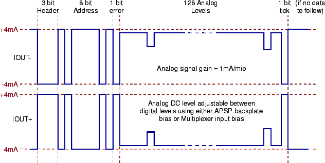
Then, a data frame is sent to the output, starting at the position where a tick mark
would be issued otherwise. Fig. shows such a frame, which starts
with a header of three bits with logic high level.
The readout processor can thus identify a data frame by searching for at least two samples
of logic high level in the output stream.
, p. ).
Then, a data frame is sent to the output, starting at the position where a tick mark
would be issued otherwise. Fig. shows such a frame, which starts
with a header of three bits with logic high level.
The readout processor can thus identify a data frame by searching for at least two samples
of logic high level in the output stream.
An eight bit address identifying the pipeline
cell follows. The pipeline column locations are numbered in a specific scheme inspired by the
Gray Code.
A set of chips running on the same clock and trigger lines ought to have synchronous
pipeline addresses, allowing to identify a chip error (e.g., by a single event upset, see
section , p. ), by an address mismatch. Moreover,
the address can be used to tag the output data in case of a known bad pipeline location.
After the address, a single bit is sent which may indicate an error. The internal chip logic
watches read and write pointers of the pipeline buffer and checks if their distance
equals the latency setting. If this is not the case, a ``latency error'' occurred and the
error bit is set. Moreover, a ``FIFO error'' is produced when the FIFO, which stores the
addresses of pipeline cells containing data to be read out, is full.
After sensing an error in the data frame, the type of error can be read over the ![]() bus.
Errors are cleared by a (soft or hard) reset applied to the APV25.
bus.
Errors are cleared by a (soft or hard) reset applied to the APV25.
After header, address and error bit,
the analog data of all 128 channels are transmitted in multiplexed order.
The overall output is 140 bits wide. With ![]() or
or ![]() output modes, the
output frame exactly replaces four or two tick marks including the interval following the pulse.
Thus, a tick mark follows immediately after an output frame except when another trigger
is pending. In that case, the first data frame is immediately followed by another one.
output modes, the
output frame exactly replaces four or two tick marks including the interval following the pulse.
Thus, a tick mark follows immediately after an output frame except when another trigger
is pending. In that case, the first data frame is immediately followed by another one.