


Next: APV25 Circuit Details
Up: Strip Tracker Electronics
Previous: Strip Tracker Electronics
Contents
APV
The APV chip series was developed as a front-end amplifier for the CMS silicon strip tracker.
It includes a preamplifier and shaper, an analog pipeline and a deconvolution filter
for each of its 128 channels.
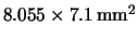
Figure:
Block diagram of the APV chip. The schematics to the left
of the 128:1 multiplexer (MUX) is implemented individually for each of the 128 channels.
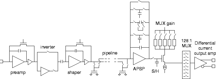 |
Fig. ![[*]](crossref.gif) shows the internals of the APV chip [46].
After the integrating preamplifier, the signal polarity can be selected by optionally
inserting an inverter. The CR-RC shaper has a peaking time of
shows the internals of the APV chip [46].
After the integrating preamplifier, the signal polarity can be selected by optionally
inserting an inverter. The CR-RC shaper has a peaking time of  . Feedback resistors
of both preamplifier and shaper as well as bias currents and voltages are programmable.
The output of the shaper is sampled with the bunch crossing frequency of
. Feedback resistors
of both preamplifier and shaper as well as bias currents and voltages are programmable.
The output of the shaper is sampled with the bunch crossing frequency of  (corresponding to a period of
  ) and
fed into a pipeline of adjustable length. At the end of the pipeline, the signals are
extracted upon a trigger request. When the chip is configured for deconvolution, a
switched capacitor filter (APSP) performs the three-weight deconvolution method as
described in section , p. . Alternatively, a single sample of the shaper output
is extracted directly. A sample/hold (S/H) stage and an amplifier with programmable gain follow.
Finally, the signals of all 128 channels are multiplexed onto a single line with a differential
current amplifier output. Moreover, an internal calibration circuit allows to test the
functionality of each channel.
) and
fed into a pipeline of adjustable length. At the end of the pipeline, the signals are
extracted upon a trigger request. When the chip is configured for deconvolution, a
switched capacitor filter (APSP) performs the three-weight deconvolution method as
described in section , p. . Alternatively, a single sample of the shaper output
is extracted directly. A sample/hold (S/H) stage and an amplifier with programmable gain follow.
Finally, the signals of all 128 channels are multiplexed onto a single line with a differential
current amplifier output. Moreover, an internal calibration circuit allows to test the
functionality of each channel.
The current and final version of the APV chip series is called APV25S1, which is manufactured
in the
 submicron process as its predecessor APV25S0. The earlier APV6
version [47]
basically had the same functionality, but was produced in the Harris AVLSIRA process.
There were also a DMILL version called APVD and
an adapted APVM chip with longer shaping time and current monitoring capabilities for MSGC readout.
The following enumeration gives an overview of the APV chip development [48].
submicron process as its predecessor APV25S0. The earlier APV6
version [47]
basically had the same functionality, but was produced in the Harris AVLSIRA process.
There were also a DMILL version called APVD and
an adapted APVM chip with longer shaping time and current monitoring capabilities for MSGC readout.
The following enumeration gives an overview of the APV chip development [48].
 Harris AVLSIRA radiation hard CMOS
- 1993 - APV3 -
- 1995 - APV5 - 128 channels with addition of analog multiplexer
- 1996 - APV6 -
- 1998 - APVM - Development of APV6 into MSGC read-out chip
 TEMIC DMILL radiation hard CMOS
- 1997-99 - APVD - development of DMILL versions
-
IBM Deep Submicron CMOS
- 1999-2000 - APV25 - Redesign
The most important distinction between the APV25 and its predecessors is a significantly improved noise
performance. Moreover, the number of pipeline cells was increased from 160 to 192.
Nonetheless, the die size could be decreased due to the smaller structures of the submicron
process (fig. ). Moreover, this transition implied a reduction in the supply
voltages from
 (APV6) to
 (APV25).
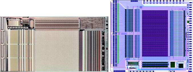
Figure:
The die layout of APV6 (
 , left) and
APV25S1 (
, left) and
APV25S1 (
 , right) front-end
chips. Both chips are shown seven times larger than in reality. The 128 input pads are visible
on the left edges, the large central parts are covered by the pipeline and the control
and output pads are to the right.
, right) front-end
chips. Both chips are shown seven times larger than in reality. The 128 input pads are visible
on the left edges, the large central parts are covered by the pipeline and the control
and output pads are to the right.
 |
Subsections
Next: APV25 Circuit Details
Up: Strip Tracker Electronics
Previous: Strip Tracker Electronics
Contents
Markus Friedl
2001-07-14