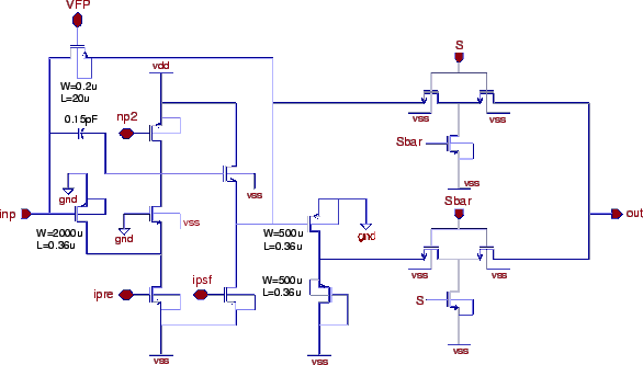
The integrating preamplifier circuit (fig. ![[*]](crossref.gif) ) is composed of
a single-ended folded cascode amplifier with a feedback
capacitor of
) is composed of
a single-ended folded cascode amplifier with a feedback
capacitor of ![]() and an input transistor of pFET type with a size
of
and an input transistor of pFET type with a size
of
![]() . Its large effective width results from a poly-gate structure,
where many smaller gates are arranged in parallel [52,34], since
it turns out that such a design is the best choice with respect to intrinsic noise [35].
The nominal bias current of the input stage is
. Its large effective width results from a poly-gate structure,
where many smaller gates are arranged in parallel [52,34], since
it turns out that such a design is the best choice with respect to intrinsic noise [35].
The nominal bias current of the input stage is ![]() .
.
The output is connected to a source follower, which provides the voltage shift required for
stable DC operation through the feedback resistor, which is realized as transistor of variable
conductance. As pointed out in section , p. , the ohmic feedback avoids drifts and
pileup effects. A unity gain inverter follows the preamplifier. With the two
mutual switches, either the direct or the inverted output is sent to the shaper stage.
While the direct output is intended for use with n-bulk detectors, the inverted output
is intended for p-bulk detectors, which produce current pulses of opposite polarity.
Since the dynamic range of the shaper is limited, its working point is not
centered between the supply voltages. The optional inverter between preamplifier and shaper thus allows
linear operation with input signals of either polarity. To avoid parasitic feedthrough in a switch,
the center of the two transistors is pulled to ![]() in the off condition.
The nominal gain of the preamplifier is
in the off condition.
The nominal gain of the preamplifier is
![]() (
(
![]() )
with a single channel power consumption of
)
with a single channel power consumption of
![]() , which is the predominant contribution of the total chip.
Source follower and inverter stages each dissipate
, which is the predominant contribution of the total chip.
Source follower and inverter stages each dissipate ![]() .
.
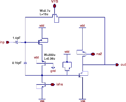
The CR-RC shaping filter (fig.
) with a time constant of
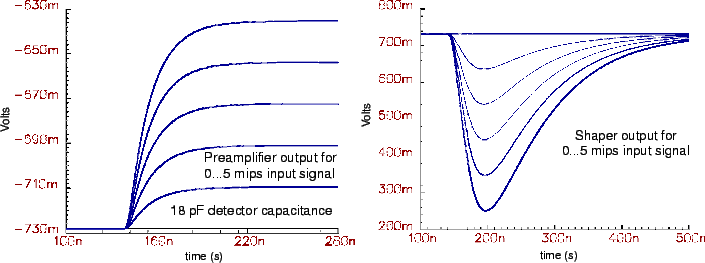 |
shows a SPICE simulation of preamplifier and shaper
output with an input charge of