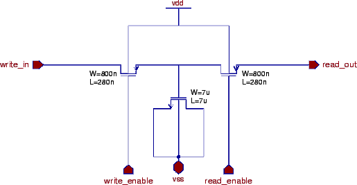
The shaper output is sampled at clock intervals
and stored in the analog pipeline, which is actually realized
as a ring buffer of 192 cells with cycling write and read pointers.
Their distance determines the latency time between particle signal and trigger arrival.
With a clock frequency
of ![]() , the maximum time allowed for this trigger decision is more than
, the maximum time allowed for this trigger decision is more than ![]() ,
well covering the CMS first-level trigger delay of
,
well covering the CMS first-level trigger delay of ![]() .
After receiving a trigger, it takes more than
.
After receiving a trigger, it takes more than ![]() to send all pipeline data to the
output line through a multiplexer.
To protect valuable information from being overwritten, a FIFO with a depth of 32
locations stores the pipeline addresses of those cells waiting for readout.
These marked cells are then skipped by the write pointer until the data are actually passed on.
In peak mode, only a single sample is retained, which corresponds to the maximum of the CR-RC
shaping curve when clock and trigger latency are properly adjusted.
Three cells are marked in deconvolution mode for later processing by the APSP.
This procedure avoids dead time while keeping a serial readout scheme.
to send all pipeline data to the
output line through a multiplexer.
To protect valuable information from being overwritten, a FIFO with a depth of 32
locations stores the pipeline addresses of those cells waiting for readout.
These marked cells are then skipped by the write pointer until the data are actually passed on.
In peak mode, only a single sample is retained, which corresponds to the maximum of the CR-RC
shaping curve when clock and trigger latency are properly adjusted.
Three cells are marked in deconvolution mode for later processing by the APSP.
This procedure avoids dead time while keeping a serial readout scheme.
Fig.
![[*]](crossref.gif) shows one of the
shows one of the