While it is possible to build a discrete amplifier for a single or few channels,
the huge number of readout channels in high energy physics experiments demands high integration.
Present front-end chips usually include 128 separate amplifier channels
together with analog bias generators, sample/hold circuits, the associated control logic and
a multiplexing output stage. In some cases, a pipeline storage or a digitization circuit are
included as well. All of these functions are built into an integrated circuit (IC)
with a die size of less than ![]() .
.
Since a semiconductor detector produces a current signal, the amplifier must have
a low-resistance current input. The shape of the current pulse depends
on the bias voltage (see section ![[*]](crossref.gif) , p. ). There are specialized fast low-noise amplifiers
which can visualize the current waveform [30], but usually it is more convenient
to measure the integrated current, which corresponds to the collected charge.
Thus, the first stage of the amplifier is an integrator. As the MIP charge is only 22500 electrons,
special attention must be paid to noise minimization, which is done by a special filter
(``shaper'') in the second stage of the amplifier.
, p. ). There are specialized fast low-noise amplifiers
which can visualize the current waveform [30], but usually it is more convenient
to measure the integrated current, which corresponds to the collected charge.
Thus, the first stage of the amplifier is an integrator. As the MIP charge is only 22500 electrons,
special attention must be paid to noise minimization, which is done by a special filter
(``shaper'') in the second stage of the amplifier.
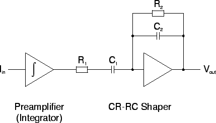 |
shows the principal schematics of an integrating preamplifier
together with a CR-RC shaper. With equal resistors, capacitors and thus time constants
gives a good approximation for that case.
Since the input current pulse is always
much shorter than the shaping time constant, it can be approximated by a
Dirac-![]() pulse weighted with the collected charge
pulse weighted with the collected charge ![]() .
The amplifier response to such an input is
.
The amplifier response to such an input is
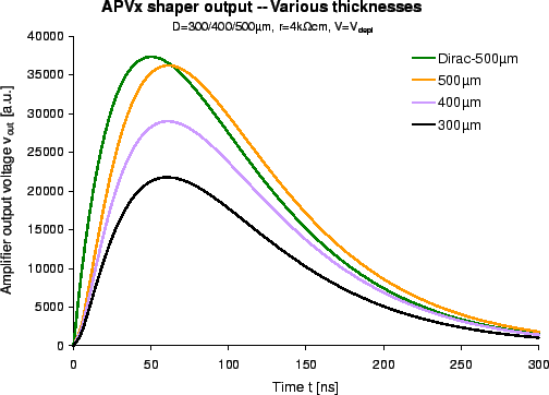
The simulation discussed in section , p. , has been used to feed an integrating
preamplifier with CR-RC shaper with the calculated detector currents and compare
the output to the one obtained with an idealized Dirac-![]() input pulse (eq. ).
A shaping time of
input pulse (eq. ).
A shaping time of ![]() , which is also used in the APV amplifier for CMS, was chosen.
The simulated amplifier output waveforms with silicon detectors of
, which is also used in the APV amplifier for CMS, was chosen.
The simulated amplifier output waveforms with silicon detectors of ![]() ,
, ![]() and
and ![]() thickness are compared to a Dirac-
thickness are compared to a Dirac-![]() input pulse in fig. .
input pulse in fig. .
 |
In practice, the preamplifier has a resistor feedback in addition to the integrating capacitor so its output smoothly returns to zero. Thus, drift and saturation are avoided without disturbing the principal function. However, the time constant of feedback capacitor and resistor must be small enough to avoid pile-up effects with frequent signals.
The preamplifier input, as seen from the detector, is capacitive when neglecting the feedback
resistor. Its value is given by the feedback capacitor (typically around
![]() ) multiplied by the open-loop gain (typically
) multiplied by the open-loop gain (typically ![]() ), leading to a typical input
capacitance of
), leading to a typical input
capacitance of ![]() . The detector signal current is divided between
the strip (or pixel) capacitance and the amplifier input capacitance, so their ratio should be
as high as possible towards the amplifier. Taking the above values with a typical strip
detector (
. The detector signal current is divided between
the strip (or pixel) capacitance and the amplifier input capacitance, so their ratio should be
as high as possible towards the amplifier. Taking the above values with a typical strip
detector (![]() ), the charge loss is
), the charge loss is ![]() and thus negligible.
and thus negligible.