Next: Radiation Damage
Up: Silicon Sensors
Previous: Energy Loss
Contents
Charge Collection
The ionization of particles traversing the detector leads to the creation of free
electron-hole pairs as discussed in the previous section.
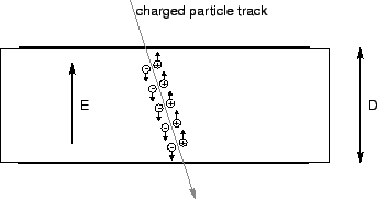
Fig. ![[*]](crossref.gif) shows the principal layout of a solid state detector with
opposite electrodes.
shows the principal layout of a solid state detector with
opposite electrodes.
Figure:
A charged particle traversing the detector generates
free electron-hole pairs along its track, which are moved by the electric field.
 |
An electric field between the electrodes is required to move these carriers
according to the relation
 |
(2.4) |
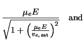
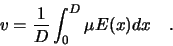
where is  is the mean carrier drift velocity,
  the mobility and
  the electric field.
The mobilities and thus drift velocities are different for electrons
and holes. The linear relation of eq. is only valid for weak electric fields;
at high electric field strength, the increasing number of collisions of the carriers with the
crystal lattice finally leads to saturation of the average velocity.
For silicon, empirical functions have been found for electrons and holes [14,15],
the electric field.
The mobilities and thus drift velocities are different for electrons
and holes. The linear relation of eq. is only valid for weak electric fields;
at high electric field strength, the increasing number of collisions of the carriers with the
crystal lattice finally leads to saturation of the average velocity.
For silicon, empirical functions have been found for electrons and holes [14,15],
where
 and
denote the saturation velocities, which are
in the order of
and
denote the saturation velocities, which are
in the order of
 .
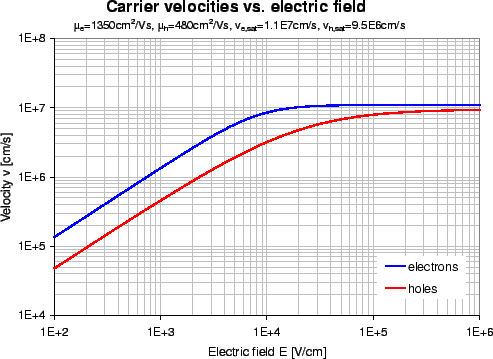
These general relations for electron and hole velocities are graphically shown in
fig. .
.
These general relations for electron and hole velocities are graphically shown in
fig. .
Figure:
Electron and hole velocities vs. the
electric field strength in silicon.
 |
While the charges move inside the detector bulk, a current is induced in the electrodes,
no matter whether the carriers finally reach the electrodes or not.
This current  is proportional to the sum of all carrier velocities [16],
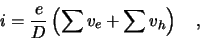 |
(2.6) |
with the elementary charge  and the detector thickness
  . The integrated current gives
the total collected charge
. The integrated current gives
the total collected charge  , which is usually measured with integrating and thus charge-sensitive
amplifiers,
, which is usually measured with integrating and thus charge-sensitive
amplifiers,
 |
(2.7) |
After the generation of a free electron-hole pair, the electron
moves to the positive electrode while the hole moves to the negative.
If no charges are trapped, the sum of the
distance they travel equals the detector thickness, regardless of their initial position.
Thus, the integral term in eq. equals the detector thickness multiplied by the number
of pairs  , and the total collected charge is
 |
(2.8) |
The collected charge is stated in terms of electrons, which might mislead to the
false conclusion that only the electrons contribute to the charge measured at the electrode.
In fact, both electrons and holes are responsible for the charge collection in equal parts,
since on average both carriers travel through half of the detector if no charge trapping
occurs.
In usual silicon detectors, virtually all charges finally reach the electrodes.
After heavy irradiation however, charge traps emerge
such that the mean travel distance shrinks. In other solid state detector materials, such as
diamond [17] or gallium arsenide [18], charge traps are always present,
resulting in a mean pair travel distance less than the detector thickness.
The charge collection efficiency  can thus be expressed by the mean travel distance,
which is also called ``charge collection distance''
can thus be expressed by the mean travel distance,
which is also called ``charge collection distance''  , divided by the detector thickness,
 |
(2.9) |
Depending on the sensor material, the electric field can be homogeneous or not.
Diamond detectors merely consist of a thin film with ohmic contacts on both sides.
An applied voltage results in a homogeneous field between the electrodes.
With silicon however, it is impossible to operate a detector this way, because the
intrinsic number of free carriers due to thermal excitation would be orders of magnitude
higher than the expected detector signal. Thus, one either has to cool down the sensor
to very low temperature or introduce a reverse-biased pn-junction, which
is obviously more practical.
A junction is introduced by doping with acceptors and donors resulting in zones
of p and n types. Starting with a homogeneously doped material, a thin layer
with a high doping density of the other type is applied onto the surface, resulting in
a pn-junction. On the opposite surface, which is known as backplane, the bulk type doping
is enhanced to get a good ohmic contact.
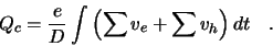
Fig. shows the schematic layout of a silicon detector based on
n-type bulk material, which is mostly used. Once the junction is under reverse bias,
all free carriers in the bulk are drained by the electric field. The
thickness of the implants with high doping concentration ( and
and  ) is in the
order of a micrometer, so that the difference between bulk and total detector thickness
is negligible.
) is in the
order of a micrometer, so that the difference between bulk and total detector thickness
is negligible.
Figure:
Schematic cross-section of a silicon detector with
implant thicknesses not to scale. The electric field results from a bias
voltage above the depletion voltage.
 |
The bulk donor (or acceptor) density  can be obtained from its resistivity
  . In the
case of an n-type bulk the relation is
. In the
case of an n-type bulk the relation is
 |
(2.10) |
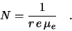
The electric properties in a one-dimensional detector model are illustrated
by fig. . Backplane and implant thicknesses are neglected and
an abrupt junction is assumed.
Figure:
Charge density, electric field and potential
in a one-dimensional model of a silicon detector at full depletion.
 |
When the pn-junction is fully
depleted (i.e. there are no free carriers in the bulk), only the core excess
charges of donors and acceptors
remain, such that the charge densities of bulk
 and implant
 are
are
 |
(2.11) |
The bulk charge density is constant over the full width of the bulk.
Since the global charge must be balanced in a steady state, positive and negative
charges have to match. This condition is leads to the width  of constant
non-zero implant charge density which is equal to the bulk width but scaled down by the ratio of
doping concentrations,
of constant
non-zero implant charge density which is equal to the bulk width but scaled down by the ratio of
doping concentrations,
 |
(2.12) |
The charge density  can be obtained by the Poisson equation
 |
(2.13) |
with the dielectric constant  .
In the case of full depletion, the electric field is of triangular shape,
rising from zero at the backplane (
.
In the case of full depletion, the electric field is of triangular shape,
rising from zero at the backplane ( ) to its maximum at the
junction (
) to its maximum at the
junction ( ). In the implant, the field quickly drops to zero again.
The maximum electric field
). In the implant, the field quickly drops to zero again.
The maximum electric field  is given by
 |
(2.14) |
The relation
 |
(2.15) |
defines the electric potential  .
The potential difference between backplane and implant electrodes is the voltage
.
The potential difference between backplane and implant electrodes is the voltage  applied
to the detector. At full depletion,
applied
to the detector. At full depletion,  is given by
 |
(2.16) |
If the applied voltage is higher than the depletion voltage, a constant offset adds to
the electric field as shown in fig. . With
 ,
the electric field can be approximately considered constant.
When the applied voltage is below full depletion, the field does not extend over the
whole bulk. With its maximum still at the junction, only a fraction of the sensor
is depleted. Obviously, the charge collection is inefficient in that case, since the
carriers do not move outside
the electric field. The width of the depletion zone, or collection distance
,
the electric field can be approximately considered constant.
When the applied voltage is below full depletion, the field does not extend over the
whole bulk. With its maximum still at the junction, only a fraction of the sensor
is depleted. Obviously, the charge collection is inefficient in that case, since the
carriers do not move outside
the electric field. The width of the depletion zone, or collection distance  , is given by
 |
(2.17) |
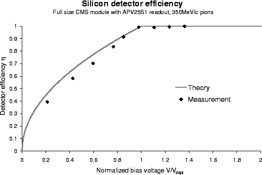
Thus, the efficiency of a silicon detector is given by
 |
(2.18) |
Fig. compares the theoretical efficiency (eq. ) to
measurement [12].
Figure:
Theoretical and measured efficiency of a silicon detector.
While theory suits well at depletion and above, it does not perfectly describe
the low voltage regime.
 |
In a homogeneous electric field, the carrier velocities are constant. Initially all carriers
move towards the electrodes and gradually they are drained at the electrodes until
all charges are gone. As the mobilities of electrons and holes differ,
the current waveform is a superposition of two triangles of the same area, but different
slope.
In silicon detectors however, the behavior is different because the
electric field depends on the position and moreover, the carrier velocities are on the edge
of saturation. For a better understanding of the influence of
the various parameters, the current waveform has been simulated [19,20]
based on the above model including the nonlinear velocities (eq. ).
The movement and resulting currents of both electrons and holes are calculated
in finite time steps.
Figure:
Electron and hole currents induced by a MIP in a standard
silicon detector (
 ,
,
 )
at the depletion voltage and at
)
at the depletion voltage and at
 .
.
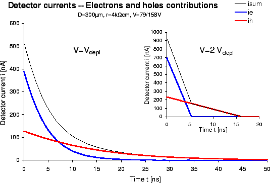 |
Fig. shows the current contributions of electrons and holes in
a standard silicon detector at and at  .
Neglecting the nonlinear velocities and the quantization of the carriers,
it can be shown that the electron component follows an exponential decay at full depletion.
A single electron starting at the junction () moves according to
.
Neglecting the nonlinear velocities and the quantization of the carriers,
it can be shown that the electron component follows an exponential decay at full depletion.
A single electron starting at the junction () moves according to
 |
(2.19) |
Substituting the velocity with eq. and using a linear dependence of the
electric field on the position, one gets the differential equation
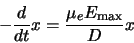 |
(2.20) |
with the solution
 |
(2.21) |
using the initial condition .
In the case of twice the depletion voltage as shown in the insert of fig. ,
the current shapes are approximately linear since the electric field is almost constant.
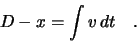
Figure:
Currents induced by a MIP in silicon detectors
(
) of various thicknesses (
 )
at their depletion voltages (
)
at their depletion voltages (
 ).
).
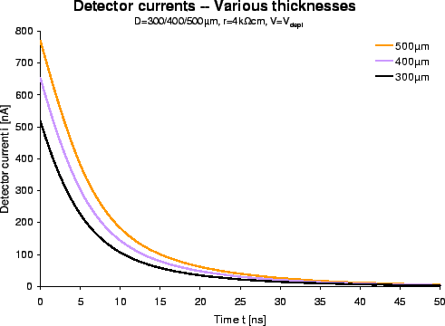 |
Fig. shows the sum current of detectors with various thicknesses
at their respective depletion voltages, which scale with the square of the thickness (eq. ).
The current waveforms approximately scale with the thickness. Although the distances, which
the carriers have to travel, are farther, the higher electric field results in faster
movement. If the linear relationship between electric field and carrier velocities (eq. )
held, the collected charge would exactly scale with the detector thickness at the respective
depletion voltage.
The overall drift time  is given by
 |
(2.22) |
The velocity will be substituted with the integral average of eq. over  ,
,
 |
(2.23) |
With the linear dependence of the electric field on the position, we get
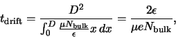 |
(2.24) |
which is independent of the thickness.
Although the maximum electric field in silicon detectors of  to
to
 touches the
saturation region of the carrier velocities, the nonlinear influence is not yet dominant, as
seen in fig. . Thus, the benefit of silicon detectors thicker than the
canonical
touches the
saturation region of the carrier velocities, the nonlinear influence is not yet dominant, as
seen in fig. . Thus, the benefit of silicon detectors thicker than the
canonical  is an approximately proportionally higher signal output.
Next: Radiation Damage
Up: Silicon Sensors
Previous: Energy Loss
Contents
Markus Friedl
2001-07-14