The Front-End Driver (FED) receives and digitizes the analog data of multiple APVs. Moreover, it extracts the data frames out of the stream and processes the signals.
The current prototype of the FED [59] is realized in the PMC format with eight
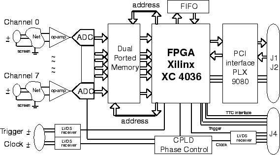
electrical input channels and a PCI interface. Fig. ![[*]](crossref.gif) shows the block
diagram of the FED-PMC.
shows the block
diagram of the FED-PMC.
The analog inputs are digitized by 10 bit ADCs (of which 9 bits are read out) at ![]() .
Similar to the PLL ASIC, the sampling time can be adjusted within a clock period
for optimum sampling performance.
After a trigger is received, a programmable number of samples is stored in a dual port memory (DPM).
The data are then fetched by the Xilinx FPGA unit for further processing.
Currently, only the frame search is implemented which extracts
header, address, error bit and channel data of an APV frame and
passes them on to the PCI interface for readout.
In future versions, also signal processing such as channel reordering,
pedestal subtraction, common-mode correction,
zero-suppression and clustering algorithms will be included in the FPGA to reduce the amount of
data.
.
Similar to the PLL ASIC, the sampling time can be adjusted within a clock period
for optimum sampling performance.
After a trigger is received, a programmable number of samples is stored in a dual port memory (DPM).
The data are then fetched by the Xilinx FPGA unit for further processing.
Currently, only the frame search is implemented which extracts
header, address, error bit and channel data of an APV frame and
passes them on to the PCI interface for readout.
In future versions, also signal processing such as channel reordering,
pedestal subtraction, common-mode correction,
zero-suppression and clustering algorithms will be included in the FPGA to reduce the amount of
data.
The final FED will be a 9U VME board including analog optical receivers for 96 channels,
a TTCrx receiver for clock and trigger input and a high-speed interface (DAQ link) to the
subsequent event builder.
The overall input data rate of the final FED will be ![]() , which will
be condensed to about
, which will
be condensed to about ![]() at the DAQ link output.
at the DAQ link output.