FEC and CCU are the building blocks of the digital control path of the CMS Silicon Strip Tracker. They are responsible for the transmission of clock and trigger signals from the control room to the front-end electronics. Moreover, control commands and readback values are transmitted in both directions.
The Front-End Controller (FEC) receives the clock and trigger information from an integrated TTCrx receiver. Moreover, it has a control bus interface for communication. The present prototype of the FEC is built in the PMC (PCI Mezzanine Card) form factor with a PCI interface, while the final FEC will be a VME module of 9U height.
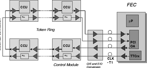
A single FEC is connected to a number of Communication and Control Units (CCUs)
in a token ring network topology (fig. ![[*]](crossref.gif) ).
The CCUs in such a ring are located close to each other within the silicon tracker, while
the connection to the control room is made through the digital optical link.
).
The CCUs in such a ring are located close to each other within the silicon tracker, while
the connection to the control room is made through the digital optical link.
In the ring, a token is initially sent out by the FEC and passed on from one station (CCU) to the next. A node which wants to send data replaces the token by a data frame, which is forwarded until received by the FEC, where the packet is modified and passed on until it returns to the sender. This node verifies the FEC acknowledgement and a checksum. If the transmission was successful, an empty token is inserted in the ring instead of the data frame; otherwise, the data packet is resent.
The token ring architecture minimizes the connections needed between the stations, but
relies on the functionality of all links. If a single connection is broken, the whole
ring is out of control. To overcome this risk, the final configuration of the CMS tracker control
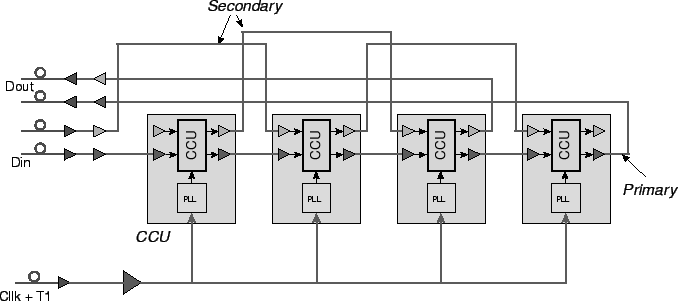
token ring will be redundant in a way that there is a second, staggered ring. Each station will have
two interfaces and automatically detect which one is in the currently active ring.
Fig. shows such a redundant network, which is
invulnerable to a single connection or CCU failure.
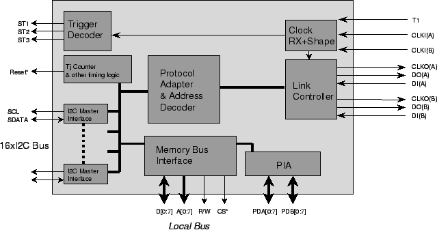
The building blocks of the CCU are shown in fig.
.
The CCU receives the combined clock and trigger signal and passes it on the PLL.
Moreover, it implements a 16 channel
Each CCU module will include a PLL chip for clock and trigger separation. These signals are
sent to an LVDS fanout ASIC. Groups of ![]() , clock, trigger and reset signals
are then distributed to each front-end module through interconnect boards.
, clock, trigger and reset signals
are then distributed to each front-end module through interconnect boards.