The analog optical link is used to transmit the multiplexed APV output to the control room, where it is digitized and processed by the FED.
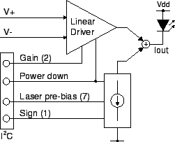
On the transmitter boards (analog optohybrid), two or three lasers are fed by the Laser Driver ASIC [55]. This chip receives analog signals from the APVMUX and converts them to a current suitable for the lasers. The block diagram of the Laser Driver is shown in fig.
![[*]](crossref.gif) .
Since the optical output power of semiconductor lasers is zero below a certain threshold,
the Laser Driver generates a programmable bias current which is added to the input related current.
Typically, a bias current slightly above the threshold is selected for optimum linearity
and noise performance at low power consumption. Moreover, four different gains of the
amplifier can be selected. The Laser Driver settings
are programmed over its , p. ) and a
readable status register reflects SEU detection.
.
Since the optical output power of semiconductor lasers is zero below a certain threshold,
the Laser Driver generates a programmable bias current which is added to the input related current.
Typically, a bias current slightly above the threshold is selected for optimum linearity
and noise performance at low power consumption. Moreover, four different gains of the
amplifier can be selected. The Laser Driver settings
are programmed over its , p. ) and a
readable status register reflects SEU detection.
The radiation to which the transmitters are subjected causes an increase in the laser threshold and a small reduction in gain. Both effects can be compensated by proper programming of the Laser Driver.
On the receiver side, the optical signal will be detected by a pin diode with an amplifier. These components will be integrated in the FED.
The specifications of the analog optical link are compared with own measurements performed
on a prototype link in section , p. .