In autumn 1999, we received a prototype of the analog optical link with four channels.
It consists of a laser driver optohybrid, which converts electrical to optical signals
with a bias programmable over its ![]() interface. On the other end of approximately
interface. On the other end of approximately
![]() of a 4-way optical fiber, a receiver hybrid provides an electrical output.
of a 4-way optical fiber, a receiver hybrid provides an electrical output.
The bias of the semiconductor laser was selected to achieve the best linearity in the specified input range while minimizing the power consumption. The optical link characteristics were tested by measuring the electrical output while applying a defined input.
![[*]](crossref.gif) gives an overview of the final specifications [69] and the HEPHY
measurements, all of which are
well within the specifications, although the prototype was designed with
slightly different requirements: it had an electrical input range of
gives an overview of the final specifications [69] and the HEPHY
measurements, all of which are
well within the specifications, although the prototype was designed with
slightly different requirements: it had an electrical input range of
As mentioned above, the bias was selected to get a linear input-output relation within the
specified input range. The laser threshold can be visualized when exceeding this input range
towards lower values. Fig. shows the input-output characteristics of all four
channels with a doubled input span.
Towards the left edge, the laser threshold is exhibited, while at high input the receiver begins
to saturate. Thus, nonlinearity occurs on either side of the nominal input window.
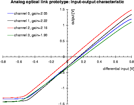 |
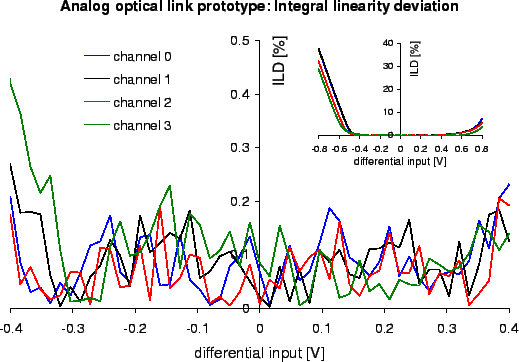
Fig. shows the integral linearity deviation of the four channels, which is
defined as the full-scale-normalized error one makes when, for a given link output signal
y, the link input signal is assumed to be the linearized value instead of the real value.
 |
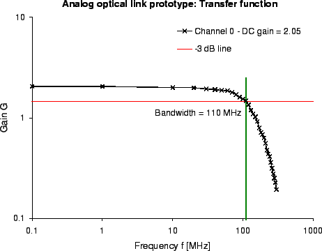
The transfer function of the analog optical link was measured with an
oscillator generating a sine wave of defined amplitude and frequency.
The oscillator output was converted to a differential signal and sent into the
optical link transmitter. Both input and output amplitudes were measured as a function
of frequency, with their ratio defining the gain.
From the transfer function (fig. ), a ![]() bandwidth
of
bandwidth
of ![]() can be extracted. With this frequency response, the effect of transients
on the APV output signal is negligible.
can be extracted. With this frequency response, the effect of transients
on the APV output signal is negligible.
 |
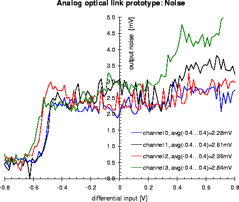
Apart from linearity, the noise figure, which is dominated by the
laser contribution, plays an important role for the analog optical link.
The output noise has been measured by the VME-ADC with an analog bandwidth ![]() and
with a digital oscilloscope at several bandwidth limits. As the ADC measurement perfectly
fits into the oscilloscope measurements, the ADC values have been scaled to represent the noise
obtained at
and
with a digital oscilloscope at several bandwidth limits. As the ADC measurement perfectly
fits into the oscilloscope measurements, the ADC values have been scaled to represent the noise
obtained at ![]() .
.
Fig. shows the optical link noise vs. the input voltage, where the ADC noise is already subtracted.
At the low edge, the optical output of the laser is zero, and thus
the remaining noise (approximately ![]() ) is attributed to the receiver part.
When the laser is turned on, its noise slightly increases with rising input voltage.
The signal-to-noise ratio given in tab. has been obtained by dividing
the full range input span (
) is attributed to the receiver part.
When the laser is turned on, its noise slightly increases with rising input voltage.
The signal-to-noise ratio given in tab. has been obtained by dividing
the full range input span (![]() ) by the average noise referred to the input.
) by the average noise referred to the input.
The noise of the analog optical link has been modelled and systematically studied with respect to device tolerances [70]. The measured noise behavior could be well reproduced by the model.
Apart from timing and crosstalk characteristics, the electrical power consumption
of transmitter and receiver sections and the noise contribution in an APV6 system were measured.
With the APV6, no difference in noise between copper cable and the optical link prototype
could be observed, since the APV6 noise is quite high
and the noise of the optical link prototype is lower than that of the final one due to the
gain reduction.
In the target system, using the APV25 and the final optical link, the latter will contribute
approximately ![]() of noise referred to the APV input.
of noise referred to the APV input.