The PLL-Delay chip has to provide clock and trigger signals with adjustable delay.
Both signals are propagated to the front-end on a single line. They are mixed such that
a clock pulse is omitted when a trigger occurs as shown in fig. ![[*]](crossref.gif)
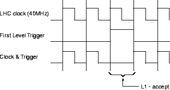 |
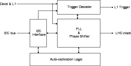
Fig.
displays the building blocks of the PLL-Delay.
To restore the full clock without missing pulses, a phase-locked loop circuit is employed as
indicated by the name of chip. The difference between input and output signals of the PLL is
the recovered trigger.
Moreover, the circuit includes a clock phase shifter. This task is performed by a voltage
controlled oscillator (VCO) composed of 12 delay cells which generate 12 different clock
phases evenly distributed within half a clock period. These phases are inverted to fill
the other half period, while an automatic calibration unit tunes the PLL circuit.
Thus, 24 taps are offered to select a fine delay in steps
of
Fine and coarse delay are programmable over the ![]() interface. For protection against
single event upsets (SEUs) caused by the radiation, the PLL-Delay uses triple-voting.
Thus, a memory cell value is validated by the majority vote of three single cells.
When a mismatch between three such cells is encountered, a status register is set
which can be read by
interface. For protection against
single event upsets (SEUs) caused by the radiation, the PLL-Delay uses triple-voting.
Thus, a memory cell value is validated by the majority vote of three single cells.
When a mismatch between three such cells is encountered, a status register is set
which can be read by ![]() . In that case, the chip is still fully functional but
the next SEU occurring on the same cell triplet will definitely cause an unwanted condition.
To avoid such an error, the chip should be reprogrammed soon after a SEU is indicated in
the status register.
. In that case, the chip is still fully functional but
the next SEU occurring on the same cell triplet will definitely cause an unwanted condition.
To avoid such an error, the chip should be reprogrammed soon after a SEU is indicated in
the status register.