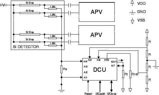
The Detector Control Unit is monitoring low voltages, the detector current and temperature.
Fig. ![[*]](crossref.gif) shows the its function on a silicon detector module.
A small resistor is inserted in the ground connection of the polysilicon resistors
to measure the voltage drop which scales with the detector leakage current.
Four equal resistors between the supply rails, tapped at
shows the its function on a silicon detector module.
A small resistor is inserted in the ground connection of the polysilicon resistors
to measure the voltage drop which scales with the detector leakage current.
Four equal resistors between the supply rails, tapped at ![]() and
and ![]() ,
are used to monitor the supply voltages. Moreover, an external NTC thermistor measures
the silicon detector temperature, while an integrated temperature sensor monitors the DCU
chip temperature.
,
are used to monitor the supply voltages. Moreover, an external NTC thermistor measures
the silicon detector temperature, while an integrated temperature sensor monitors the DCU
chip temperature.
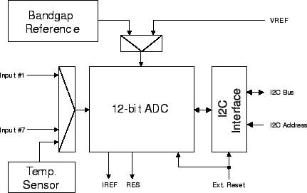
The DCU architecture is shown in fig.
.
Seven inputs and the internal temperature sensor are multiplexed onto an ADC with 12 or optionally
14 bits resolution.
The reference voltage for the ADC is generated normally from an internal bandgap diode,
but can be overridden by an external source for test purposes.
The ADC is implemented in a single slope
serial architecture, where a linear ramp is obtained by charging or discharging a
capacitor with a constant current. The analog input voltage is compared with the linear
ramp and a counter, which is fed from the