The Silicon Strip Tracker (SST) of the CMS experiment covers an area of ![]() ,
which makes it the largest silicon detector under construction. The sensors are arranged
in a total number of about 20000 modules, which consist of one or two strip detectors in series
together with the associated readout electronics. Depending on the position within CMS, the geometry
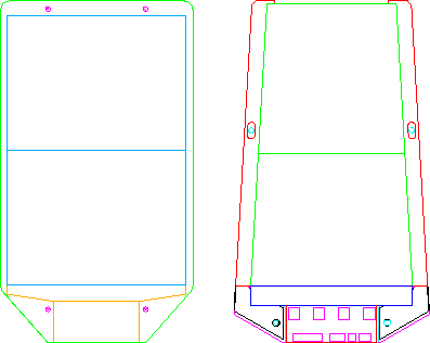
of the sensors and the number of readout strips varies: In the barrel region, the sensors
are rectangular, while the endcap sensors are of trapezoidal shape to fit together in discs
(fig.
,
which makes it the largest silicon detector under construction. The sensors are arranged
in a total number of about 20000 modules, which consist of one or two strip detectors in series
together with the associated readout electronics. Depending on the position within CMS, the geometry
of the sensors and the number of readout strips varies: In the barrel region, the sensors
are rectangular, while the endcap sensors are of trapezoidal shape to fit together in discs
(fig. ![[*]](crossref.gif) ).
).
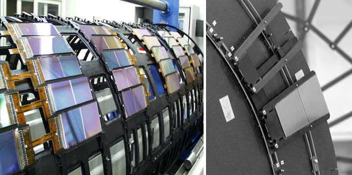 |
. To allow
better area coverage, the modules will overlap like roof tiles, which causes a tilt
angle of , p. ).
In the disks (right part of fig. ) however, there is no Lorentz
shift and thus no tilt, since electric and magnetic fields have the same direction.
A carbon fiber frame holds one or two silicon sensors which are connected to the readout hybrid via a pitch adapter. Each module has 512 or 768 strip channels which are read out by four or six chips, respectively. On both ends of the frame, cooling pipes are sinking the heat produced by sensors and electronics.
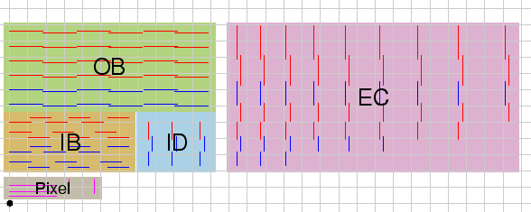 |
shows the functional groups of the CMS silicon tracker.
The ten strip layers in the barrel are divided
into the inner barrel (IB) and the outer barrel (OB), which are numbered in ascending
order with the radius. The seven rings of the disk modules
are divided into the inner disks (ID) and the endcaps (EC), again numbered with ascending radius.
The properties of the barrel and disk silicon detectors
are given in tab. and , respectively.
|
The acceptance criteria for the silicon detectors of the CMS tracker have been worked out in great detail [42], where the most important specifications common to all sensors are:
, p. ) are considered not yet known well
enough and thus implicate a certain risk.
gives an overview of the detector specifications.
The inner barrel modules will be fabricated either of two chained 4" wafers or of a single
6" wafer resulting in the same total area. Since the inner part is exposed to a higher radiation
dose, its sensors are made of low-resistivity material which reach the inversion point at higher
fluence (see section , p. ). The outer modules, which are a replacement of the
previous MSGC design, have longer strips, resulting in an increased capacitive load. As pointed out in
section , p. , this implies a higher noise figure. To restore a reasonable signal-to-noise
ratio (
In the innermost layer of the CMS strip tracker,
the occupancy is approximately ![]() , decreasing to
, decreasing to ![]() in the outermost layer.
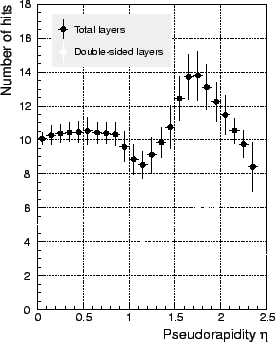
Fig. shows that every energetic particle arising from a collision traverses
between eight and fourteen
detectors in the silicon tracker [43], depending on the pseudorapidity
in the outermost layer.
Fig. shows that every energetic particle arising from a collision traverses
between eight and fourteen
detectors in the silicon tracker [43], depending on the pseudorapidity ![]() .
Double-sided layers are counted
only once. The reason why the number of radial hits can exceed the number of detector layers is
that there is some overlap between adjacent sensors to ensure full coverage, which occasionally
results in two hits in the same plane.
.
Double-sided layers are counted
only once. The reason why the number of radial hits can exceed the number of detector layers is
that there is some overlap between adjacent sensors to ensure full coverage, which occasionally
results in two hits in the same plane.
 |
Several institutes (including the HEPHY) will assemble the CMS silicon strip detector modules
using automatic and
semi-automatic machinery. The modules will be fabricated with an internal precision of
about ![]() in the sensor plane and approximately
in the sensor plane and approximately ![]() in the coordinate
perpendicular to that plane [44]. After a mechanical survey procedure,
the absolute position of
each strip in space will be known with an accuracy better than
in the coordinate
perpendicular to that plane [44]. After a mechanical survey procedure,
the absolute position of
each strip in space will be known with an accuracy better than ![]() .
Each assembled module will be tested in regard of certain acceptance criteria
such as a limited number of bad strips. Moreover, it will be subjected to a thermal cycle
(cooling down and heating up)
to verify the robustness of the bond wires.
.
Each assembled module will be tested in regard of certain acceptance criteria
such as a limited number of bad strips. Moreover, it will be subjected to a thermal cycle
(cooling down and heating up)
to verify the robustness of the bond wires.