The high resolution pixel detector [39] is the innermost part of the CMS Tracker. Since the particle density is very high, a small-scale pixel geometry is required for unambiguous hit recognition and precise vertex reconstruction. Short-lived particles arise from the primary vertex, which can decay after having travelled only a few hundred micrometers. The pixel detector must distinguish such secondary vertices from the original collision point.
The barrel part consists of three pixel layers at radii of ![]() ,
, ![]() and
and ![]() .
The innermost layer will only be present in the
initial low-luminosity phase of LHC, since radiation damage will destroy this layer
at a later stage.
Fig.
.
The innermost layer will only be present in the
initial low-luminosity phase of LHC, since radiation damage will destroy this layer
at a later stage.
Fig. ![[*]](crossref.gif) shows the layout of the pixel detector in the 2-layer high-luminosity
configuration.
shows the layout of the pixel detector in the 2-layer high-luminosity
configuration.
The CMS pixel detector includes a total of about 45 million pixels with a cell size
of
![]() . A grid of
. A grid of ![]() pixels is read out by
a custom ASIC [40,41] called DM_PSIxx (where
xx is the version number).
Currently, the chip is manufactured in radiation hard DMILL technology by
Temic [36], but the transition to the deep submicron CMOS
process is being prepared.
The readout chip incorporates a separate amplifier for each pixel cell together with an
adjustable threshold discrimination, channel multiplexing and the associated digital logic.
pixels is read out by
a custom ASIC [40,41] called DM_PSIxx (where
xx is the version number).
Currently, the chip is manufactured in radiation hard DMILL technology by
Temic [36], but the transition to the deep submicron CMOS
process is being prepared.
The readout chip incorporates a separate amplifier for each pixel cell together with an
adjustable threshold discrimination, channel multiplexing and the associated digital logic.
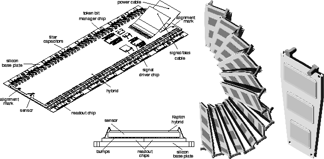
Several pixel chips together with one or more sensor tiles and a common control
logic make up a module, which is the basic building block of the pixel detector.
Fig. shows a barrel pixel module on
the left. The three pixel layers are composed of 160, 256 and 384 such modules, with an average
of 15 chips per module.
Each disk is divided into 24 blades. The right side of
fig. shows one half of a disk together with a single
blade. Each blade holds four sensors on one side and
three on the opposite side, which slightly overlap to ensure full coverage.
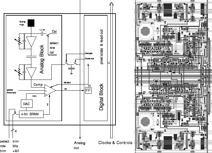 |
, including
an integrating preamplifier with CR-RC shaper stage in the analog block. A calibration
pulse can be injected over a capacitor to test the electronics, whereas the usual input
is from the pixel sensor cell. The shaper output is then sent into the comparator stage, which has
a global threshold. To deal with channel-to-channel
variations, the threshold of each individual cell can be fine-tuned with a 3-bit value
which is transformed into analog with the cell DAC. A fourth register is used to turn
off the discriminator completely which allows to switch off noisy pixels. When a PUC
reports a hit, the analog shaper output is read out using a sample/hold circuit and
stored in a buffer together with position information and a timestamp. On the arrival of
a first-level trigger, the corresponding buffer cells are coded and multiplexed onto the output line.
The die layout of two adjacent PUCs of the
DM_PSI32 prototype chip is shown on the right side of fig. . The large dots are
intended for the bump-bonding connections to the sensor.