On strip detectors, the top electrode (at the pn-junction) forms long, thin lines with a typical
spacing (``pitch'') between ![]() and
and ![]() .
In a simple readout system, where the position information is derived from the strip
with the highest signal, the root mean square (
.
In a simple readout system, where the position information is derived from the strip
with the highest signal, the root mean square (![]() ) spatial resolution
with pitch
) spatial resolution
with pitch ![]() is given by
is given by
| (2.28) |
In practice, analog signals of all channels are read out in most cases. This allows advanced signal processing which can significantly improve the spatial resolution, because the charge is shared between neighboring strips due to capacitive coupling. One possible method is to calculate the center of gravity of the analog signals for a particle's crossing point. Depending on the signal-to-noise (SNR) figure, the spatial resolution can be improved by a factor of up to ten compared to digital with sophisticated signal processing.
Normally, each strips is connected to a separate amplifier channel. In some detector designs, only every second (or even third) strip is read out, while the remaining ``intermediate strips'' are terminated with high impedance. As there is capacitive coupling, signals on these intermediate strips are partially transferred to the readout strips. With this method, the number of amplifier channels can be reduced, while the performance is naturally worse than with full readout, but still better than without intermediate strips [23].
The electrical connection between strips and amplifier channels is
made with a thin wire (typically ![]() diameter), welded onto
corresponding pads using an ultra-sonic bonding wedge.
If the sensor pitch does not match the readout chip input pad spacing,
which is usually the case, an intermediate
pitch adapter must be used.
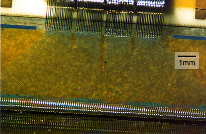
Fig.
diameter), welded onto
corresponding pads using an ultra-sonic bonding wedge.
If the sensor pitch does not match the readout chip input pad spacing,
which is usually the case, an intermediate
pitch adapter must be used.
Fig. ![[*]](crossref.gif) shows a row of wire-bonds between a silicon detector, the pitch
adapter and the readout chip.
shows a row of wire-bonds between a silicon detector, the pitch
adapter and the readout chip.
 |
The maximum size of a silicon strip detector is determined by the diameter of the silicon
single-crystal rod out of which the wafers and later the sensors are cut. Wafers of ![]() have
been used for more than a decade, while present technology allows to process
have
been used for more than a decade, while present technology allows to process ![]() wafers.
Thus, sensors of about
wafers.
Thus, sensors of about
![]() can be produced in a single piece.
For larger detectors, two or more strip detectors can be mechanically and electrically
chained together in ``ladders'', thus multiplying the effective strip length.
Ladders of
can be produced in a single piece.
For larger detectors, two or more strip detectors can be mechanically and electrically
chained together in ``ladders'', thus multiplying the effective strip length.
Ladders of ![]() active length, consisting of twelve sensors,
have been successfully built for the silicon target of the WA96 neutrino
experiment (NOMAD-STAR) [24] at CERN.
active length, consisting of twelve sensors,
have been successfully built for the silicon target of the WA96 neutrino
experiment (NOMAD-STAR) [24] at CERN.
The electrical representation of a strip is a capacitive current source,
composed of the backplane capacitance and the interstrip capacitance against neighboring strips.
A single strip typically shows a total capacitance of
![]() .
Investigations on prototypes for the CMS silicon tracker [25] revealed that
the actual value is independent on the detector thickness in the range
of
.
Investigations on prototypes for the CMS silicon tracker [25] revealed that
the actual value is independent on the detector thickness in the range
of ![]() to
to ![]() , because the interstrip capacitance increases while
the backplane part decreases and vice versa.
However, the total strip capacitance does depend on the ratio of the strip implant
width
, because the interstrip capacitance increases while
the backplane part decreases and vice versa.
However, the total strip capacitance does depend on the ratio of the strip implant
width ![]() and the pitch
and the pitch ![]() . The empirical equation
. The empirical equation
shows measured values of the
total strip capacitance as a function of 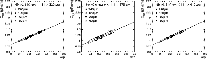 |
In practice, the primary restriction of the total strip length is the capacitive load seen by the
readout amplifier, which determines the noise figure (see section , p. ).
The strip pitch design has to consider the available budget, the required spatial resolution
and the expected particle rate,
typically aiming for a single strip hit probability (``occupancy'') of a few percent or less.