When the top electrode is made of tiled rectangular or square pads,
the charge is collected on the pad where the particle track crossed the detector.
Pad dimensions between ![]() and
and ![]() have been realized.
Small pads (typically below
have been realized.
Small pads (typically below ![]() ) are called pixels.
) are called pixels.
The spatial resolution improves with smaller pixels. A principal limitation to the
pixel size is the readout electronics, since each pixel needs its own amplifier channel.
The electrical connection between each sensor pixel and its associated readout channel is not
as easily established
as with regular strip detectors, where a bond wire is placed between each strip and the
corresponding amplifier channel (see section ![[*]](crossref.gif) , p. ).
The pixel detector geometry is two-dimensional, but
wire-bonding is restricted to one dimension. A possible solution for
large pad detectors is to route all pads to a single row of bonding pads on one side of the sensor,
as it has been done with the Silicon Detector of the PHOBOS Experiment at
RHIC [26,27].
This method reduces the connection problem to the same
procedure as with strip detectors, but it implies some disadvantages: First of all,
the capacitive and resistive loads dramatically increase, leading to a higher
noise figure, and crosstalk problems can arise. Moreover, the manufacturing of the
sensor gets complicated and thus more expensive. Such a routing solution is feasible
with a pad size in the millimeter range, but impossible for small pixels as designed for CMS.
, p. ).
The pixel detector geometry is two-dimensional, but
wire-bonding is restricted to one dimension. A possible solution for
large pad detectors is to route all pads to a single row of bonding pads on one side of the sensor,
as it has been done with the Silicon Detector of the PHOBOS Experiment at
RHIC [26,27].
This method reduces the connection problem to the same
procedure as with strip detectors, but it implies some disadvantages: First of all,
the capacitive and resistive loads dramatically increase, leading to a higher
noise figure, and crosstalk problems can arise. Moreover, the manufacturing of the
sensor gets complicated and thus more expensive. Such a routing solution is feasible
with a pad size in the millimeter range, but impossible for small pixels as designed for CMS.
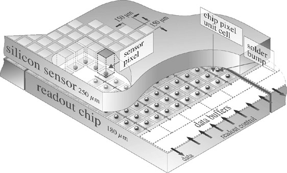
The advanced solution is to connect each pixel cell directly to the corresponding readout channel in a sandwich-like compound as shown in fig.
. Each
sensor pixel sits directly on top of the corresponding readout chip cell.
Small solder bumps (e.g. made of Indium)
are applied onto one or both sides and treated thermally before the connection is
made. Naturally, this procedure is much more complicated than wire-bonding, and
there is no possibility to inspect the bump bonds nor to repair broken connections.
Given these difficulties, one might ask why not integrate sensor and electronics onto the same wafer, since both are made of silicon? Unfortunately, the requirements for sensor and electronics grade materials are quite different in terms of bulk doping concentration, purity and operational voltage. Nevertheless, such integrated pixel devices are under development [28], where an epitaxial sensor layer of a few micrometers thickness has been grown onto a pixel chip. Prototypes were successfully operated in a beam test.