The analog behavior of the FED-PMC prototype was evaluated [73]
with respect to the digitization of multiplexed APV data.
The analog transfer characteristic of a digitizer is an important characteristic with respect to
pulse distortion and noise sensitivity. Although clocked with the system frequency of
![]() , the analog input bandwidth for pulse digitization must be considerably higher
to avoid signal loss due to slow transients.
, the analog input bandwidth for pulse digitization must be considerably higher
to avoid signal loss due to slow transients.
The transfer function of the FED has been obtained by comparing the input from a sine wave generator to the digitized output. According to the sampling theorem by H.NYQUIST5.2, analog information can only be truly reconstructed when sampled with at least twice the highest frequency contained in the analog data. If this condition is violated, aliasing effectively leads to ``mirroring'' of frequencies above half the sampling rate into the base band. Nevertheless, the amplitude of these signals reveal information about the analog performance.
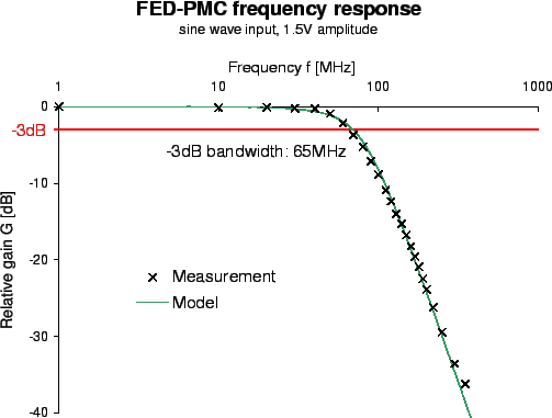 |
![[*]](crossref.gif) shows the measured transfer function of the FED-PMC,
normalized to the DC gain. A
shows the measured transfer function of the FED-PMC,
normalized to the DC gain. A 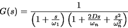 |
(5.6) |
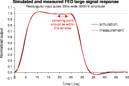
Moreover, the FED response to a rectangular input pulse with the width of one clock cycle
was measured. Such a pulse emulates an APV channel with signal information, surrounded by
pedestals. The response was measured by progressively delaying the input pulse relative to
clock and trigger in steps of ![]() , similar to the ``sequential equivalent-time sampling''
method [74] employed by some digital oscilloscopes. For comparison, the analytical
transfer function model
has been used to calculate the response to the same rectangular input pulse.
, similar to the ``sequential equivalent-time sampling''
method [74] employed by some digital oscilloscopes. For comparison, the analytical
transfer function model
has been used to calculate the response to the same rectangular input pulse.
Fig.
shows both measured and calculated FED responses to an input pulse
of
The FED noise was measured by applying stable DC voltages to the FED input. Depending on the input
voltage relative to an LSB step, we found a noise figure peaking at ![]() counts. This
includes the digitization noise and the input amplifier to approximately equal parts. Using
the nominal calibration of
counts. This
includes the digitization noise and the input amplifier to approximately equal parts. Using
the nominal calibration of
![]() , the maximum noise contribution is
, the maximum noise contribution is
![]() , referred to the input. With a full range of
, referred to the input. With a full range of ![]() ,
the noise figure corresponds to less than
,
the noise figure corresponds to less than ![]() at the APV25 input.
at the APV25 input.
Summarizing these results, the analog input stage of the FED reveals a bandwidth high enough to digitize the APV output without signal loss due to slow transients, while the FED noise contribution can be neglected compared to APV and optical link.