The same APV setup is also used for module tests with source or beam operation. In that case, several APV hybrids are read out in parallel. Thus, additional components for power and signal distribution are required as well as HV supplies for the detector bias.
Fig.
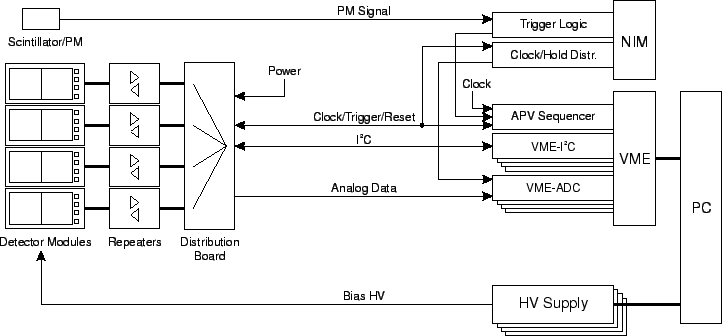
![[*]](crossref.gif) shows the extended setup for four detector modules.
The front-end electronics to the left is located in the beam area, while the
right half is located in the control room. The maximum cable length already tested between these parts
was
shows the extended setup for four detector modules.
The front-end electronics to the left is located in the beam area, while the
right half is located in the control room. The maximum cable length already tested between these parts
was
Several silicon detector modules are placed in a
particle beam. Each module needs its own repeater board, which can be either the HEPHY repeater
discussed in section , p. , or the Perugia TRI card, which has similar functionality.
Different APV versions can be mixed provided that each APV is equipped with the appropriate
repeater type. A front-end distribution board delivers power and signals to each repeater.
The particle trigger is derived from a scintillator watched by two photomultiplier (PM) tubes.
The trigger signals from the PMs are processed by standard NIM
(Nuclear Instrumentation Module) logic modules. After two independent
discriminators, the coincidence of the two PMs is formed and sent into an adjustable delay.
Its output is shaped to a short pulse of ![]() duration and fed into the APV sequencer
in the VME crate. As the sequencer input is equipped with a D-Flip-Flop, only triggers within
a small window with respect to the clock edge are accepted. This feature effectively
synchronizes the beam with the APV clock.
duration and fed into the APV sequencer
in the VME crate. As the sequencer input is equipped with a D-Flip-Flop, only triggers within
a small window with respect to the clock edge are accepted. This feature effectively
synchronizes the beam with the APV clock.
Individual VME-![]() and VME-ADC modules are intended for each detector module.
The clock returned by one of the repeaters is sent into a clock and hold distribution board,
which combines these signals in such a way that there is only a clock when the hold line is asserted.
The combined clock/hold can be delayed in three individual groups before being distributed
to the VME-ADC modules. Thus, the clock timing can be adjusted for each ADC. Experiments have
shown that the timing needs to be adjusted for different types of repeater boards and in
particular between APV6 and APV25 chips.
Naturally, analog signals from different modules can be sent into the same VME-ADC board if the timing
is compatible. Moreover, several modules can be connected to the same
and VME-ADC modules are intended for each detector module.
The clock returned by one of the repeaters is sent into a clock and hold distribution board,
which combines these signals in such a way that there is only a clock when the hold line is asserted.
The combined clock/hold can be delayed in three individual groups before being distributed
to the VME-ADC modules. Thus, the clock timing can be adjusted for each ADC. Experiments have
shown that the timing needs to be adjusted for different types of repeater boards and in
particular between APV6 and APV25 chips.
Naturally, analog signals from different modules can be sent into the same VME-ADC board if the timing
is compatible. Moreover, several modules can be connected to the same ![]() bus if
all APV chip addresses are unique.
bus if
all APV chip addresses are unique.