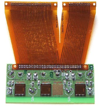
One or more APV chips are mounted on a hybrid together with decoupling capacitors and termination
resistors. Since the chips are glued and bonded, the APV footing has to match the chip version.
Two different APV25 hybrids were developed at HEPHY. Fig. ![[*]](crossref.gif) shows the
APV25S0 hybrid for up to four chips, while the other hybrid (fig. , p. )
was specifically designed for the APV25S1 irradiation test.
shows the
APV25S0 hybrid for up to four chips, while the other hybrid (fig. , p. )
was specifically designed for the APV25S1 irradiation test.
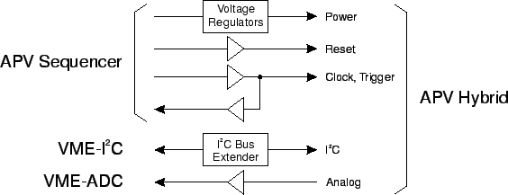
The schematic diagram of the repeater is shown in fig.
.
Local voltage regulators provide the power to the APVs, while reset, clock and trigger signals
are buffered and sent to the APV hybrid. Optionally, when using the APVMUX which includes a PLL,
clock and trigger are combined into a single signal. Moreover, clock and trigger signals are
also sent back to the VME system. The returning clock has a constant delay with respect to
the APV clock and does not depend on delay adjustments made in the APV sequencer. Thus, it is
perfectly useful for the digitization.
The ![]() bus of the APV hybrid is buffered with an extender and the levels are
adapted to those of the APV supply. Four fast amplifiers deliver the analog output of the
APVs to the VME-ADC. Once, a silicon detector module with eight APV6 chips was read out
using the analog stage of a second repeater in parallel.
bus of the APV hybrid is buffered with an extender and the levels are
adapted to those of the APV supply. Four fast amplifiers deliver the analog output of the
APVs to the VME-ADC. Once, a silicon detector module with eight APV6 chips was read out
using the analog stage of a second repeater in parallel.
Since the power supply voltages, the output stages and other details differ between APV6 and APV25 versions two different repeater boards were developed for their readout.