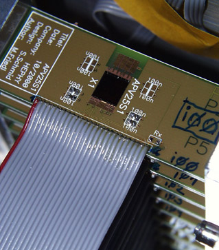
A stack of eight APV25S1 chips (fig. ![[*]](crossref.gif) ) were placed in the beam focus.
The hybrid for the chips was especially designed for this test, containing no passive elements
except decoupling capacitors. This was done because the intention was to test the APVs and
not other devices under irradiation, while the capacitors were known to be radiation tolerant.
The chips had no detector connected and the stack was placed in the cooling box at an ambient
temperature of
) were placed in the beam focus.
The hybrid for the chips was especially designed for this test, containing no passive elements
except decoupling capacitors. This was done because the intention was to test the APVs and
not other devices under irradiation, while the capacitors were known to be radiation tolerant.
The chips had no detector connected and the stack was placed in the cooling box at an ambient
temperature of
![]() .
.
 |
The APV chips were read out by the same hardware as used in module tests. For the front-end, a special backplane board was developed to connect the eight hybrids. Clock and trigger lines, which are normally terminated on the hybrid, were returned to the backplane and terminated there. An external calibration line was included but finally not used because of excess noise. An additional feature of the backplane was the possibility to monitor all supply voltages and currents.
Some of the chips should have had their output being transmitted over a new, radiation tolerant prototype of the analog optical link placed in the beam as well, but unfortunately this prototype was not fully functional, such that the data were entirely transmitted over cable.
Moreover, the PSI cyclotron system had massive problems at that time, such that only a
fifth of the targeted fluence of
![]() could be achieved -
nevertheless, good statistics and consistent data were obtained from this test.
could be achieved -
nevertheless, good statistics and consistent data were obtained from this test.
Apart from the APV25S1 chips, commercial digital optical transceivers, three silicon detector modules and submicron test structures were irradiated in this beam, but their results will not be discussed here.