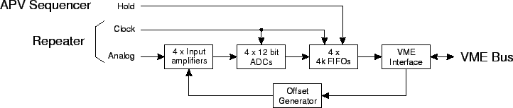
The VME-ADC (fig. ![[*]](crossref.gif) ) is used to digitize the analog data coming from the
APVs. Four input channels are amplified in the input stage and digitized by individual 12 bit ADCs
with the input clock frequency
(normally
) is used to digitize the analog data coming from the
APVs. Four input channels are amplified in the input stage and digitized by individual 12 bit ADCs
with the input clock frequency
(normally ![]() ). When a hold signal is asserted, up to 4096 samples are
stored in FIFOs, which can be read over the VME bus.
). When a hold signal is asserted, up to 4096 samples are
stored in FIFOs, which can be read over the VME bus.
The differential input range of the VME-ADC is
![]() . Although never used,
also half of this range can be selected. An individually programmable offset is added
to each channel in the input stage. Thus, the input range can
be shifted by approximately
. Although never used,
also half of this range can be selected. An individually programmable offset is added
to each channel in the input stage. Thus, the input range can
be shifted by approximately
![]() . A
. A ![]() bandwidth of
bandwidth of ![]() has been
measured for the analog inputs, which is mainly determined by one particular input amplifier.
A considerably higher bandwidth
has been achieved when omitting this amplifier at the price of less gain. This
modification was only done for the APVMUX test (see section , p. ), since its output
is clocked with
has been
measured for the analog inputs, which is mainly determined by one particular input amplifier.
A considerably higher bandwidth
has been achieved when omitting this amplifier at the price of less gain. This
modification was only done for the APVMUX test (see section , p. ), since its output
is clocked with ![]() compared to
compared to ![]() with a non-multiplexed APV.
In the latter case, two samples are obtained for each APV channel data. For optimum
digitization, the clock timing was optimized for the second sample, while discarding the first point
which is spoiled by transients.
with a non-multiplexed APV.
In the latter case, two samples are obtained for each APV channel data. For optimum
digitization, the clock timing was optimized for the second sample, while discarding the first point
which is spoiled by transients.