No irregularities were observed on the supply voltages and currents. In fact, this would only be the case with a single event latchup or gate rupture, when a conductive path between supply rails was created.
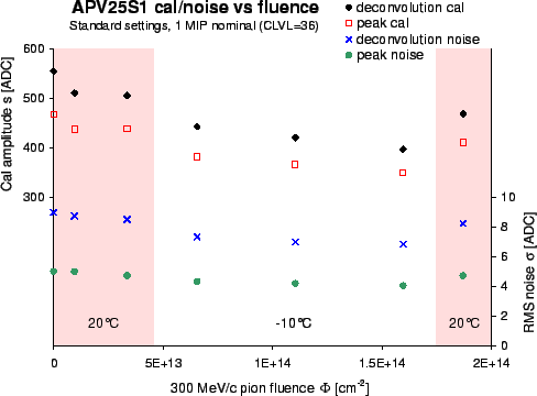 |
![[*]](crossref.gif) shows
the amplitude of the internal calibration signals in both peak and deconvolution mode
and the noise over the accumulated fluence.
The APV chips revealed a small temperature dependence, which is common for semiconductors.
Apart from that, a minor decrease in the
amplitude of about
shows
the amplitude of the internal calibration signals in both peak and deconvolution mode
and the noise over the accumulated fluence.
The APV chips revealed a small temperature dependence, which is common for semiconductors.
Apart from that, a minor decrease in the
amplitude of about The noise values however show the same development for both fluence and temperature, such that the signal-to-noise remains unaffected. Thus, this effect purely is a matter of gain. Oxide charging is the suspected reason of the gain degradation, but this is not yet confirmed and needs further investigation.